


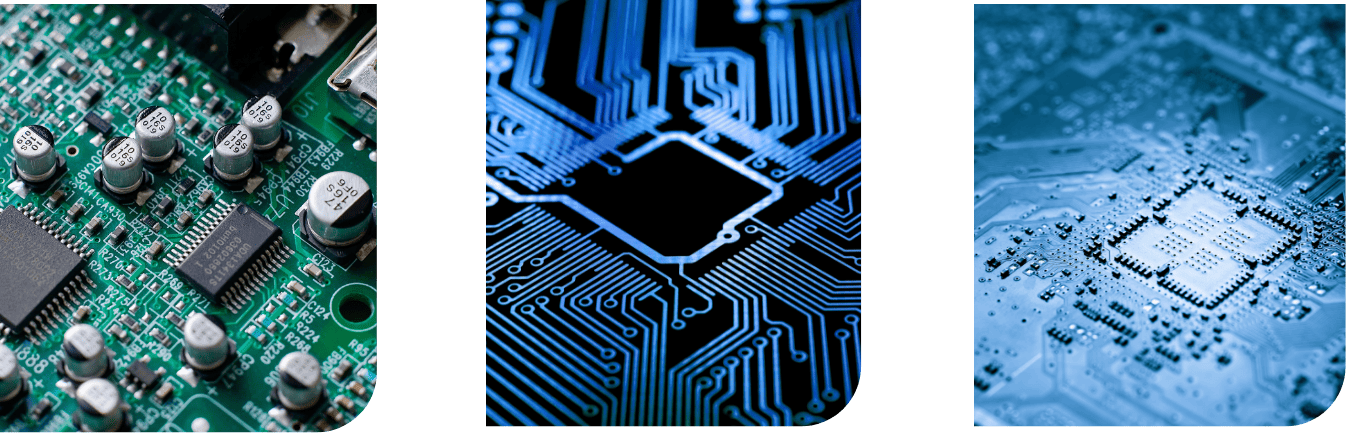
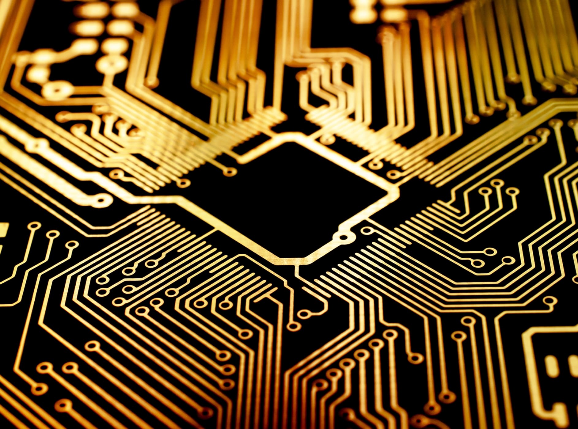
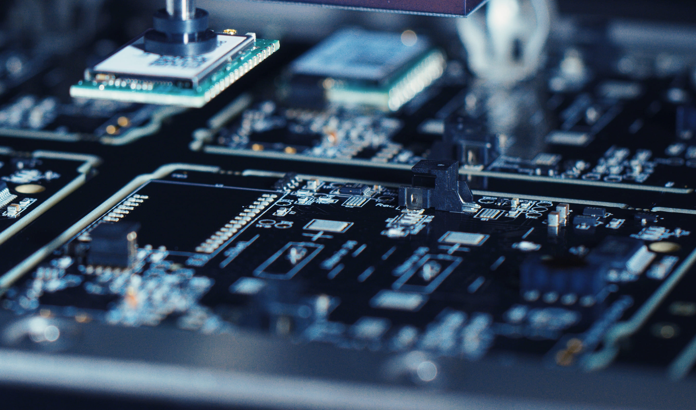
TELE-MASTER specialize in the design and production of high-quality printed circuit boards (PCBs)
Our company provides reliable PCB solutions for various industries, emphasizing advanced manufacturing technology, strict quality control, and excellent customer service. TELE-MASTER aims to support clients with competitive lead times and customized designs to meet demanding electronic applications.

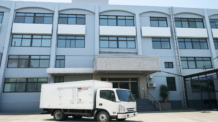
PRODUCTION LOCATIONS
1
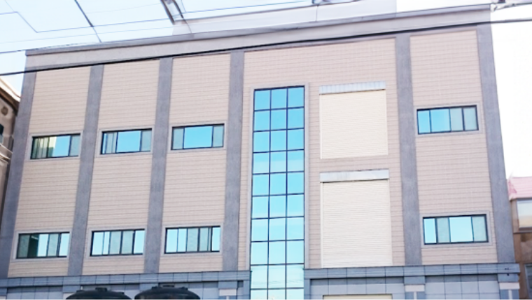
- SINCE 2000
TAOYUAN FACTORY
2
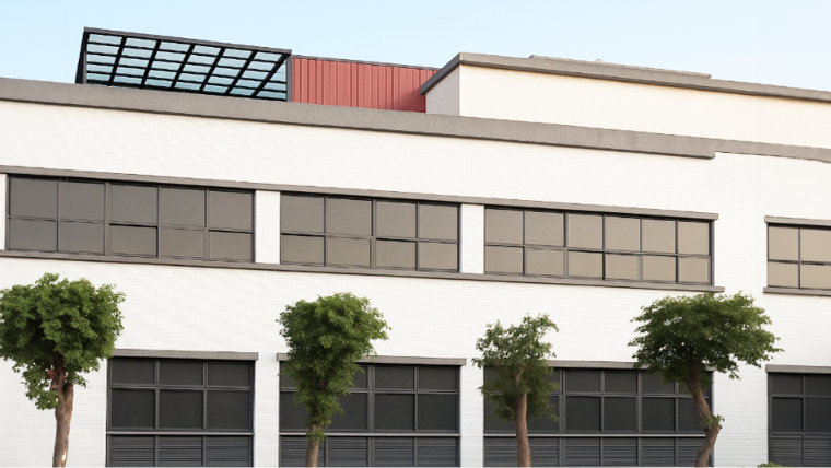
- SINCE 2023
NEW FACTORY
3
- SINCE 1990
ZHONGLI FACTORY
OUR VALUED CUSTOMERS


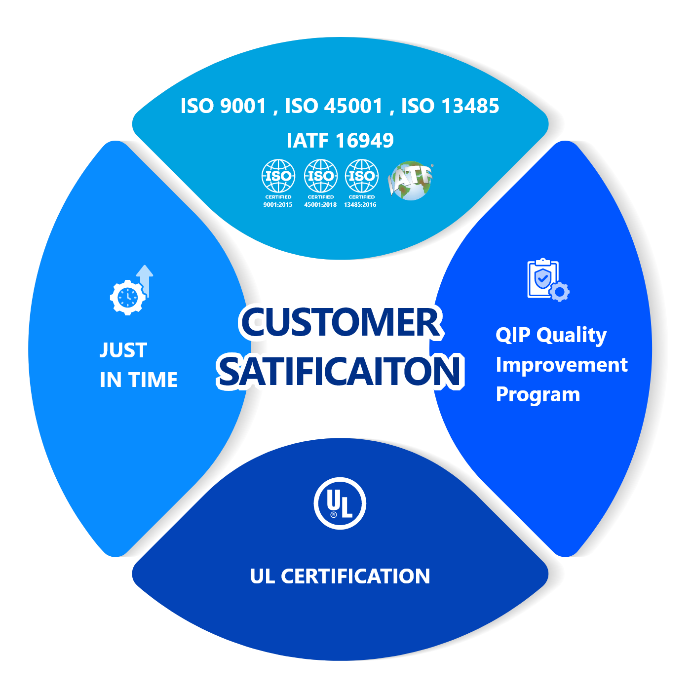
CERTIFICATION OF REGISTRATION
We have obtained the following certifications, reflecting our strong commitment to consistent,
reliable, and high-quality production you can fully trust!
UL CERTIFICATION
Certificate Of Compliance
ISO 9001:2015
Quality Management Systems
ISO 45001:2018
Occupational Health And Safety Management Systems
ISO 13485:2016
Medical Devices — Quality Management Systems — Requirements For Regulatory Purposes

IATF 16949
Automotive Quality Management System Standard
TECHNOLOGY CAPABILITY
| ITEM | DESCRIPTION |
|---|---|
| Fine Line/Pitch/Hole | Fine Line L/S: 2/2 Mils. Drilling Pitch: 19.6Mil. Via Hole: 6Mil (Mechanical), Advanced Via Hole: 4 Mils (Mechanical), |
| High Layer Counts | Min.: Single Max: 26 Layers (Advance: Max: 34 Layers) |
| Construction | Non-Regular Shapes And Constructions |
| Panel Size | Max. 24” X 40” (Working Panel) |
| Finished Board Thickness | Min.: 4Mil (0.1Mm) Max: 126Mil (3.2Mm), Special To 197Mil (6Mm) |
| Thin Core | Min. 2Mil |
| Copper Thickness | Min.: 1/4 OZ; Max.: 16 OZ (Outer Layer) |
| Copper Plating Aspect Ratio | Max.: 1:20 |
| Impedance | +/- 7% |
| HDI Board | 3+N+3 Construction |
| Material | FR4, FR5,FCCL, (Rogers, Ventec, Nelco, Arlon, Polyimide..) Further Material Request Can Be Done Per Customer Requirement. |
SURFACE FINISHED
| ITEM | DESCRIPTION | ITEM | DESCRIPTION |
|---|---|---|---|
| HASL / HAL | Available | Immersion Tin | Available |
| Nickel Plating | Available | Immersion Silver | Available |
| Gold Plating | Available | OSP | Available |
| Tin Plating | Available | Selective Gold Plating | Available |
| Immersion Gold(ENIG) | Available | Gold Finger Plating | Available |
| Immersion Gold (ENEPIG) | Available |
FPC TECHNOLOGY CAPABILITY
| ITEM | STANDARD | ENGINEERING | UNIT | REMARKS |
|---|---|---|---|---|
| Multilayer FPC | 2~4 L | 6~8 L | Um | |
| Min. Line/Space | ||||
| Inner Layer | 65/65 | 50/50 | Um | |
| Outer Layer | 75/75 | 65/65 | Um | |
| Min. Laser Via Diameter | 100 | 75 | Um | |
| Min. Laser Land | 300 | 275 | Um | |
| Min/Max. Drill Size | 150/5000 | 150/5000 | Um | |
| Min. Drill Land | 450 | 425 | Um | |
| Trace Shift Between 2 Drill Hole | 200 | - | Um | |
| PTH Size Tolerance | +/-75 | - | Um | |
| PTH Thick | <20 | - | Um | |
| OSP (Entek) | 25 | 20 | U"Inch | |
| Electrolytic Gold Plating Ni/Ag | 120~150/2~3 | - | U"Inch | |
| ENIG | 120~150/2~3 | - | U"Inch | |
| Soldermask Clearance Pad/Dam | 75/100 | 50/75 | Um | |
| Silk Spec. | +/-300 | - | Um | |
| Silk Tolerance | 150 | - | Um |

QUALITY ASSURANCE
Our engineering staff plays a pivotal role in product development and innovation, ensuring that our manufacturing process adhere to stringent quality standards.
Recognizing that quality is paramount to customer satisfaction, we are deeply committed to rigorous quality control measures and efficient manufacturing practices.
This dedication ensures that our products consistently meet the highest standards before they are introduced to the market.
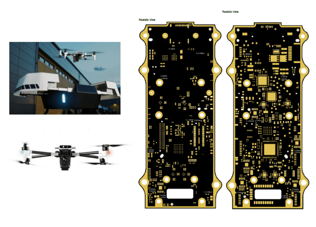
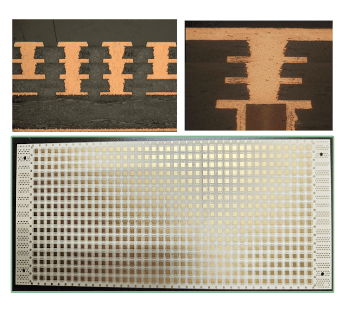
PCB PRODUCTS
HDI PCB
Material
RO4350/RO4450
| Layer | 10L |
| PNL Size | 76.2 x 186.69 mm |
| Cu Thickness | 1oz |
| Board Thickness | 1.6 mm, HDI 3+N+3, Blind via Cu filling |
| Surface Finished | ENIG |
| Application | Drone |
PCB PRODUCTS
HDI PCB
Material
RO4350/RO4450
| Layer | 8L |
| PNL Size | 76.2 x 186.69 mm |
| Cu Thickness | 1oz |
| Board Thickness | 1.6 mm, HDI 3+N+3, Blind via Cu filling |
| Surface Finished | ENIG |
| Application | Semiconductor testing board |
PCB PRODUCTS
 BLOOD ANALYZER
Thin Board PCB
Material
FR370HR
| Layer | 2 L |
| Board Thickness | 0.2 +/-0.038mm |
| Line |
Width/Space : 5/5 mil Selective Cu Plating Routing Slot 0.5Mm |
| Surface Finish | OSP + Selective Ni/120u” ,Au 3u” |
| Application | Blood analyzer |
PCB PRODUCTS
 HEARING INSTRUMENT AUDIPHONES
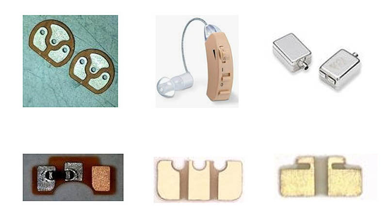
Tab PCB
Material
FPC or FR-4 halogen free material
| Layer | 1L |
| Board Thickness | 0.05~0.127 mm |
| Pcs Size | about 1.11x 1.5 mm |
| Surface Finish | Ni/100u” ,Au 2u” |
| Application | Hearing instrument , Audiphones |
PCB PRODUCTS
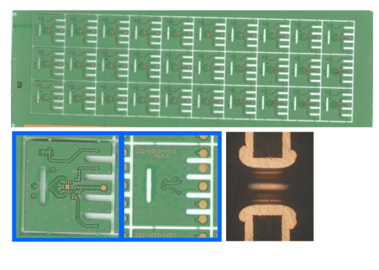
 HI FREQUENCY CONNECTOR
High Frequency PCB
Material
Nelco N4000-13 si
| Layer | 6L |
| Board Thickness | 1 +/-0.1mm |
| Line: Width/Space | 5/5 mil |
| Surface Finish | Ni/120u” ,Au 2u” |
| G/F |
Selective Au plating 30u” Blind via for L12 and L56, Buried via for L13 and L46 |
| Impedance Control | 100+/-5ohm |
| Application | Hi frequency connector |
PCB PRODUCTS
 POWER SUPPLY
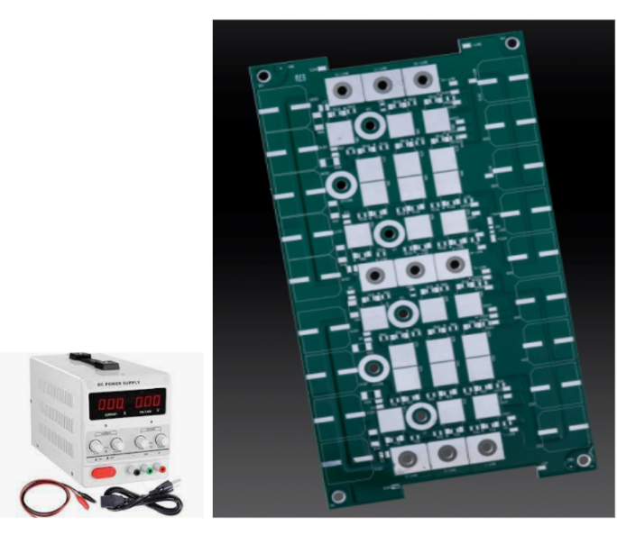
Metal Core PCB
Material
Metal Core PCB
| Layer | 2L+AL2.0mm |
| PNL Size | 4.9 x 8.75 inch |
| Cu Thickness | 2oz |
| Board Thickness | 2.4 mm |
| Thermal Conductivity | 8W / mk |
| Surface Finish | HASL |
| Application | Power supply |
PCB PRODUCTS
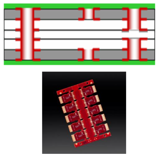
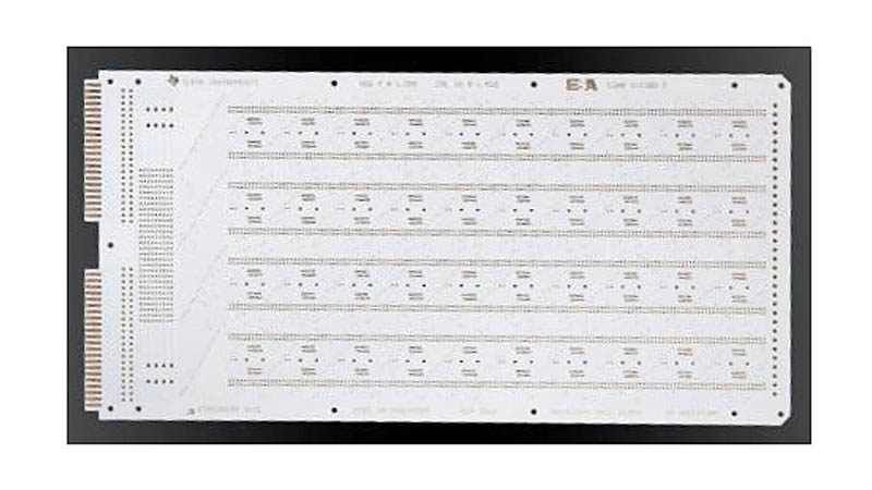
 BURN IN BOARD
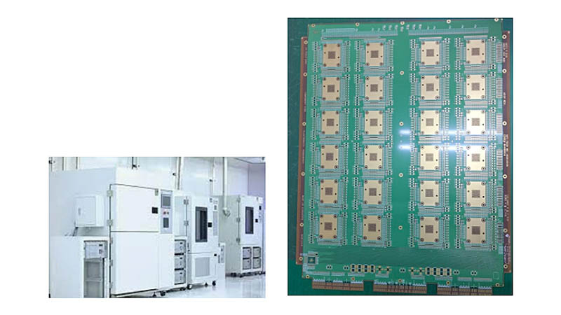
Burn In Board PCB
Material
Polyimide
| Layer | 26L |
| Piece Size | 17.7 X 22.6 inch |
| Board Thickness | 3.2 +/-0.25mm |
| Line: Width/Space | 4/4 mil |
| Surface Finish | Ni/120u” ,Au 2u” |
| G/F | Au plating 50u” |
| Drill pitch | 0.5 mm |
| Application | Burn In Board |
PCB PRODUCTS
BURN IN BOARD
Burn In Board PCB
Material
Rogers RO4350B & RO4450F
| Layer | 10L |
| Board Thickness | 2.4+/-0.24mm |
| Line: Width/Space | 5/5 mil |
| Surface Finish | Ni/120u” ,Au 2u” |
| G/F | Au plating 50u” |
| Drill pitch | 0.8 mm |
| Application | Burn In Board |

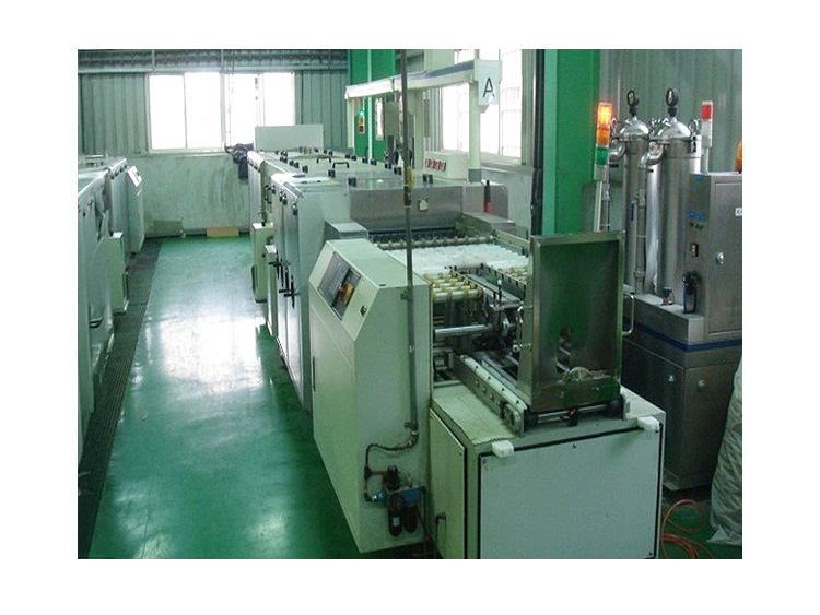
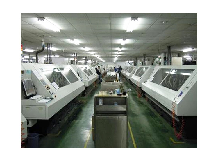
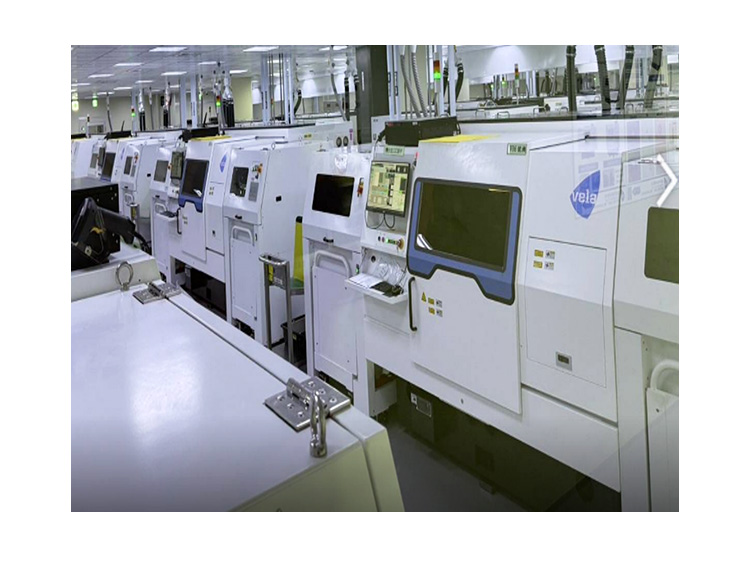
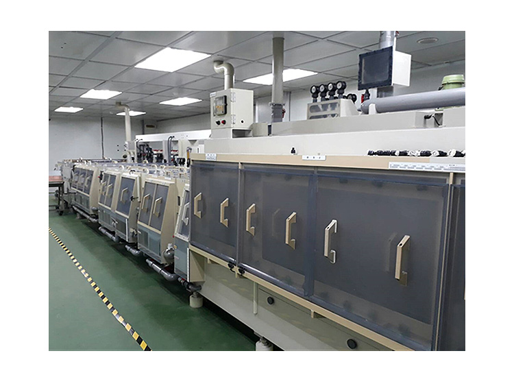
EQUIPMENT
INNER/OUTER LAYER IMAGING
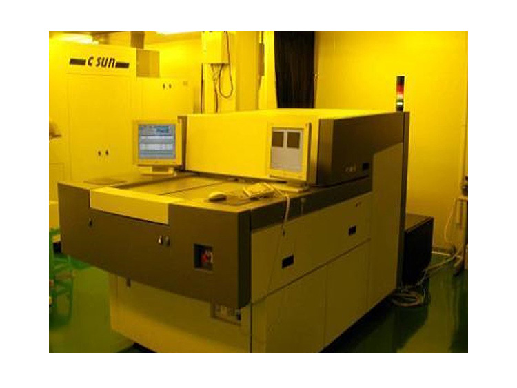
LDI 9800 (Laser Direct Imaging)
High Registration: +/- 1Mil
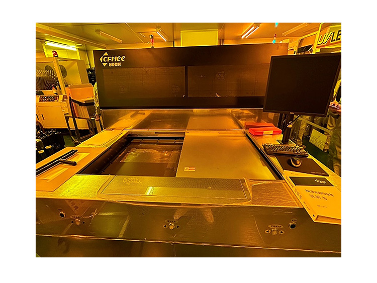
LDI MAS30T-06L20
(24X48 Inch)
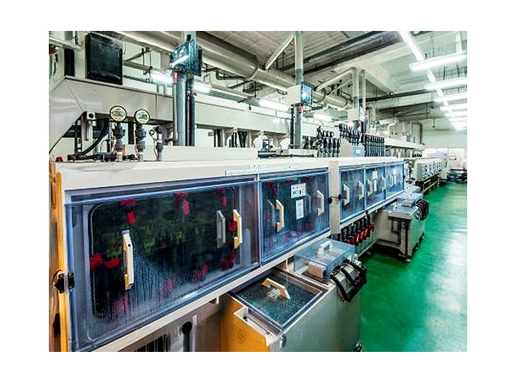
Vacuum Etching DES Line
Inline AOI
EQUIPMENT
LAMINATION
Brown/Black oxide
Lamination
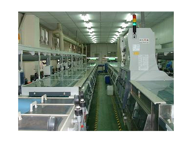
EQUIPMENT
COPPER PLATING
Cu plating pretreatment
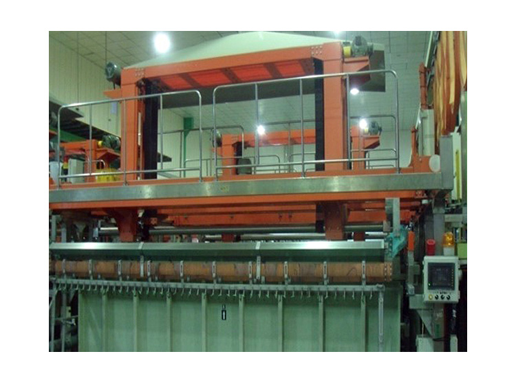
Cu plating equipment
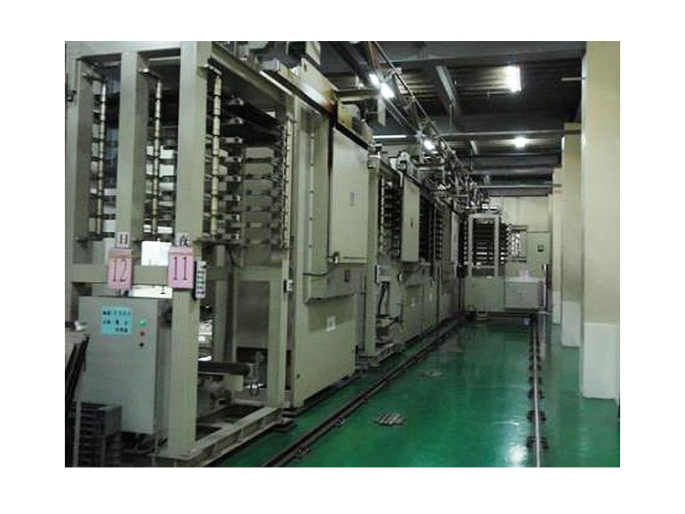
EQUIPMENT
DRILLING
Drilling machine
Laser Drilling Machine
EQUIPMENT
SOLDER MASK
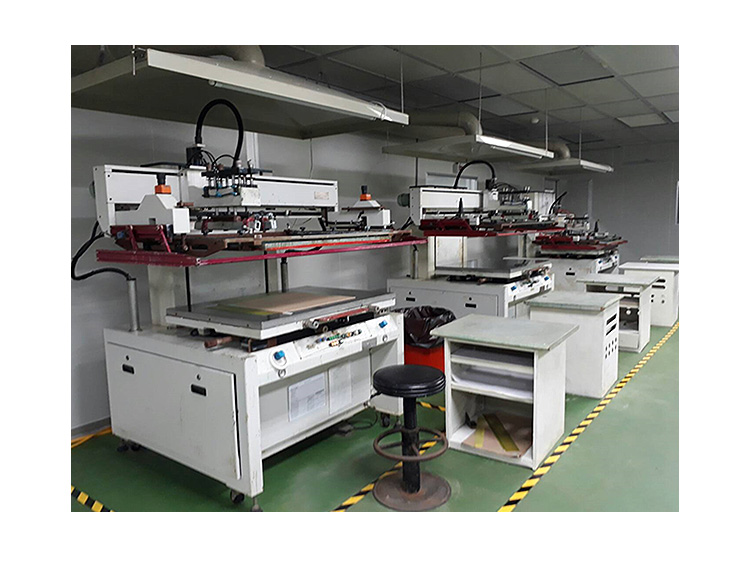
Solder Mask Coating Machine
Solder Mask Development Machine
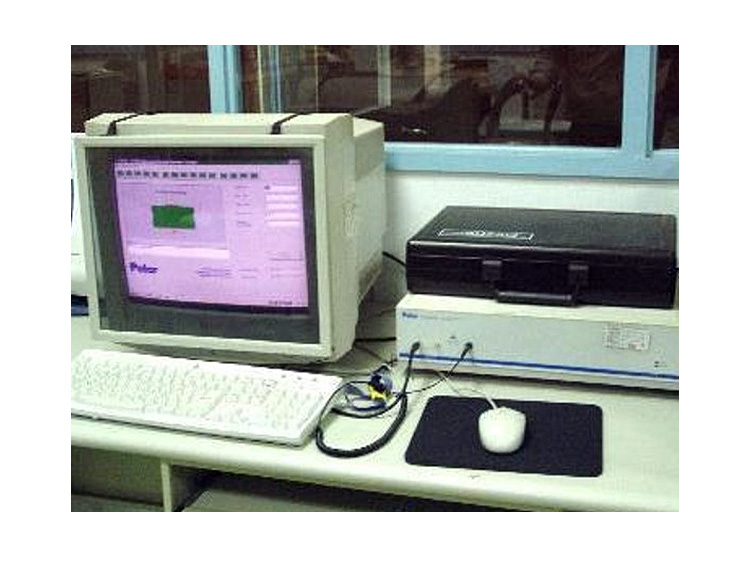
EQUIPMENT
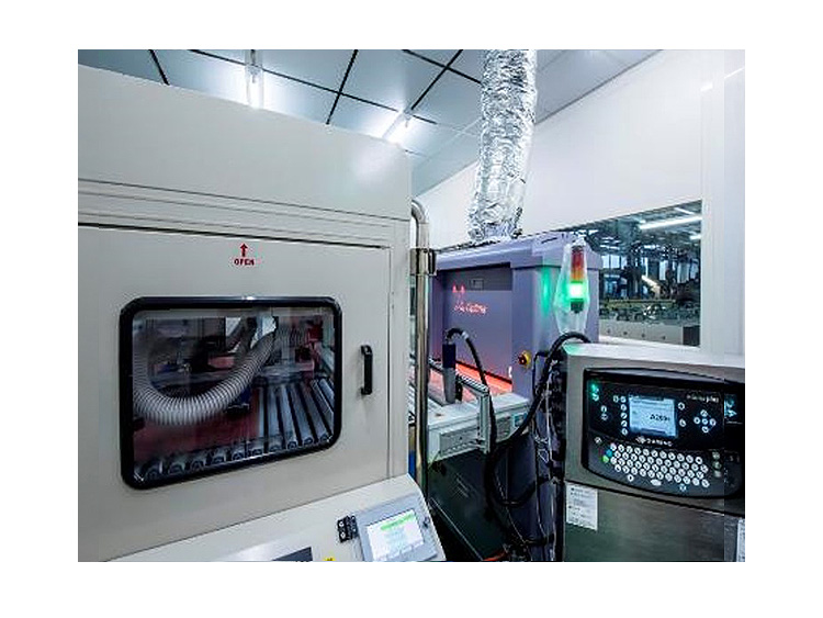
ELECTRICAL TESTING
Flying Probe Testing Machine
Flying Probe Testing Machine_ATG
EQUIPMENT
AOI & AVI & TDR
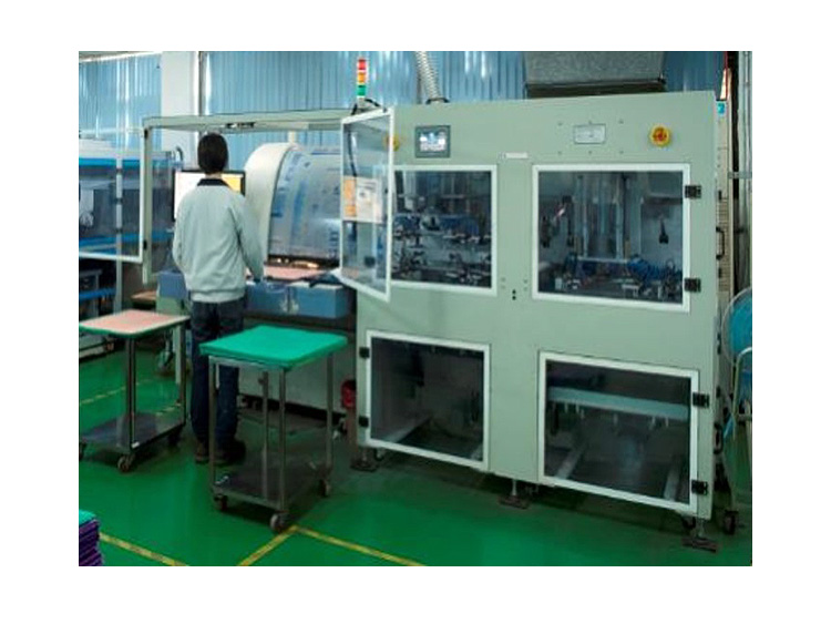
AOI
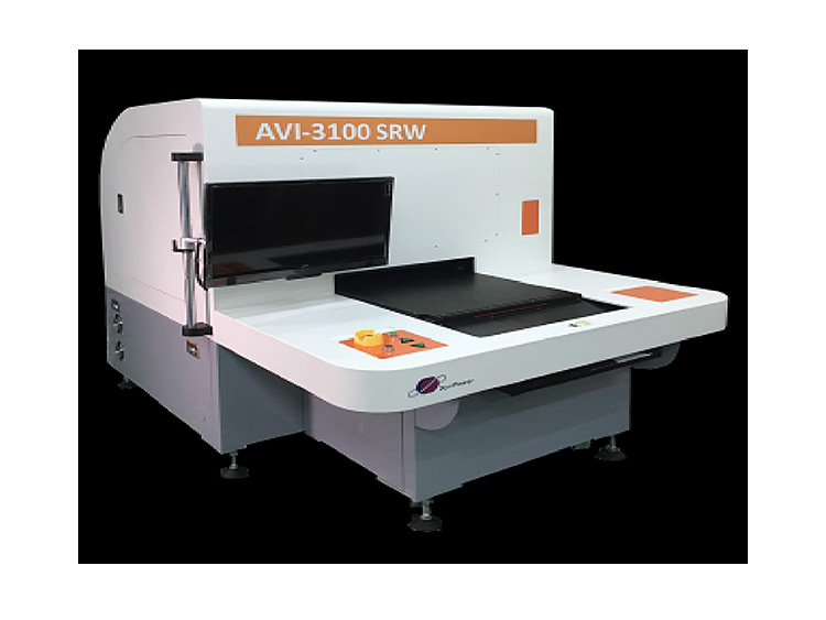
AVI
T.D.R.
Time Domain Reflector